LXF33K14 │ 4 通道 3U VPX 開發板 │ MIMO 波束成形 雷達應用 類比訊號擷取 航太應用 SDR
產品應用
- Digital Beam Forming
- MIMO Applications
- Radar waveform generators and receivers
- Telecommunicaton systems
- Experimental Physics
- Analog record and playback systems
- Aerospace and test instrumentation
- Software defined radio (SDR)
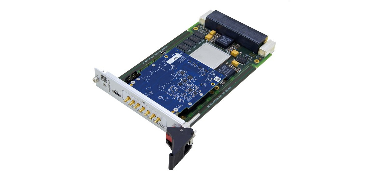
4 通道 3U VPX 16位元解析度的 310 Msps ADC / DAC
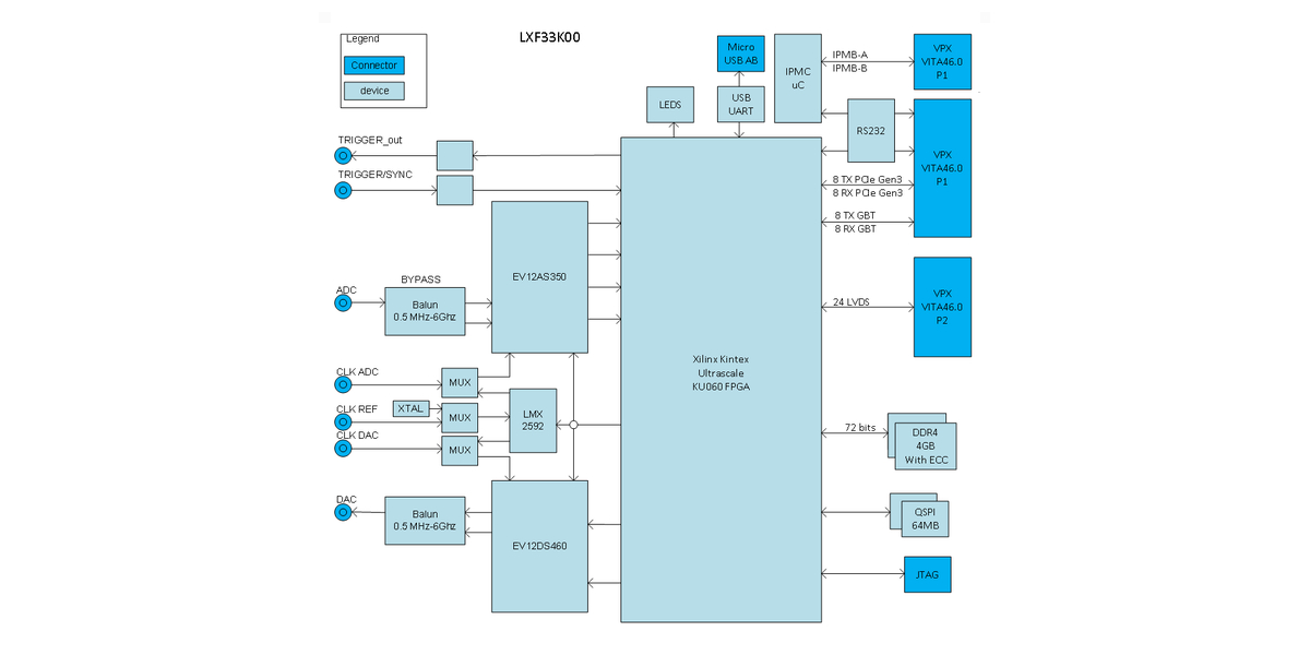
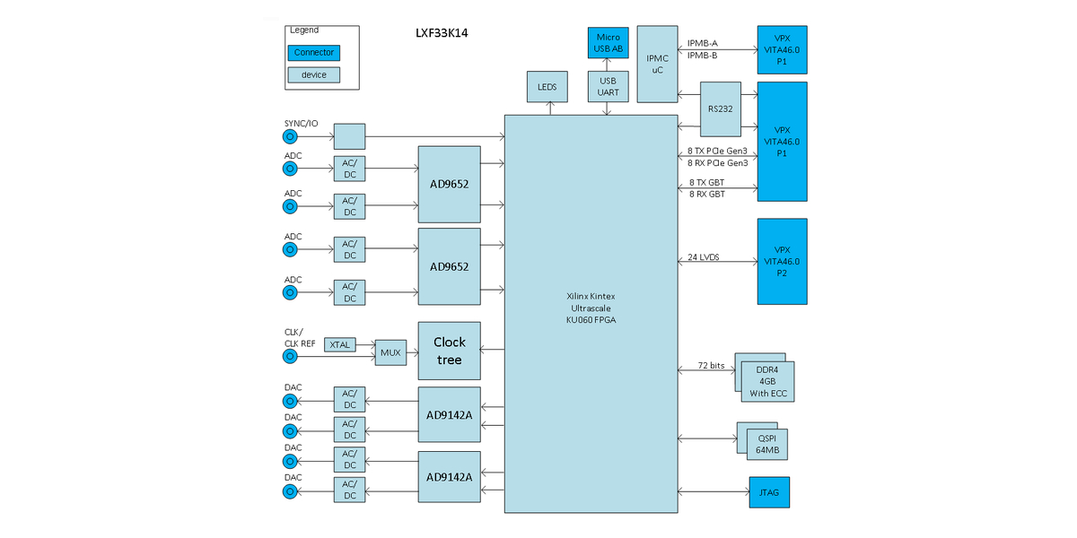
Four 16-bit A/D channels with up to 310 Msps data rate and four 16-bit D/A channels with up to 310 Msps data rate and a 1.24 Gsps update rate combined with a Xilinx Kintex Ultrascale makes the LXF33K14 the ideal platform for embedded signal processing applications such as Electronic Warfare, Wideband Radar transceiver or MIMO communication applications. The LXF33K14 is fully compliant to the Vita65.0 openVPX standard and the VITA46.11 VPX shelf management standard.
類比輸入/輸出
Depending on the application requirements it is possible to order the LXF33K14 with either a DC coupled or an AC coupled analog front end. The DC coupled interface is meant for signal acquisitions and playback in the first Nyquist zone while the AC coupled inputs also offers the option for signal acquisition and playback in the second Nyquist zone. Both the ADC and DAC offer 16-bits resolution further contributing to achieve best in class signal to noise ratios.
時脈功能
The onboard low noise clock generator ensures easy integration into small single board systems as well as standalone operation. For larger systems it is possible to easily synchronize multiple boards by providing an external reference clock. This is a special feature offered by the onboard clock pll.
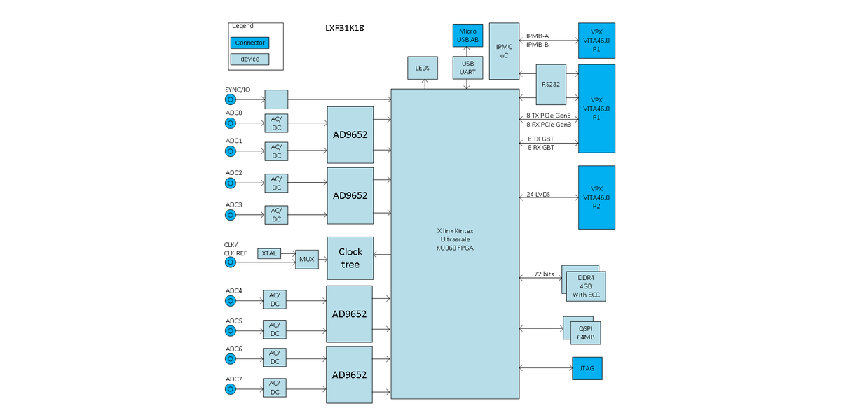
FPGA與記憶體
The LXF31K18 comprises a Xilinx Kintex Ultrascale KU060 user programmable FPGA. Most of the logic, block RAM and all DSP resources are available for customer processing. With the KU060 FPGA the LXF31K18 offers; 663 K logics cells, 1,080 36 Kbit RAM blocs, 3 PCIe interface blocks and 2,760 DSP48 slices. The FPGA speed grade is -2. The LXF31K18 FPGA connects to one 72 bits wide DDR4 memory bank, offering a total of 4GB of storage with error correction codes. At 2400 Mhz the memory bank offers a total bandwidth of 21.6 GB/s. For FPGA configuration the LXF31K18 has a 64MB QSPI FLASH memory.
VPX介面
At the P1 connector the LXF31K18 has two fat pipes that form the data plane. At the expansion plane on P1 there are also two FAT pipes. Each fat pipe can be divided into two thin pipes or four ultra thin pipes. A total of thirty-two user definable LVDS signals connect between the FPGA and the VPX P2 connector. Two types of cooling are supported by the LXF31K18. For the harsher environmental conditions, the board can be ordered in the conduction cooled version. Otherwise the board is available in an air-cooled version.
產品規格
Number of analog input channels:4
Number of analog output channels:4
Front panel IO connector type:SSMC or MMCX
Front panel IO type:ADC/DAC
Form Factor:VPX - 3U (VITA65.0 3U OpenVPX compliant)
FPGA type (3選1):
- Kintex Ultrascale - KU060 (530K logic Cells, 38Mb Block RAM, 2760 DSP slices)
- Kintex Ultrascale - KU040 (530K logic Cells, 21.1Mb Block RAM, 1920 DSP slices)
- Kintex Ultrascale - KU035 (444K logic Cells, 19Mb Block RAM, 1700 DSP slices)
Analog input specification
Input coupling (2選1):AC coupling / DC coupling
Input maximum sample rate:310 Msps
Input number of bits:16 bits resolution
Impedance:50 Ω
Input bandwidth AC coupled:10 MHz - 400 MHz
Input bandwidth DC coupledDC - 200 MHz
Input AC full scale power+6 dBm
Input DC full scale power+12 dBm
Legislation and Environmental
Supported operating temperature (2選1):Commercial (0°C ~ 70°C) / Industrial (-40°C ~ 85°C)
Ruggedization:standard Commercial Air-cooled and Rugged Conduction- cooled
ROHS Compliant:Yes - RoHS Phthalates Compliant
SVHC:Product contains no SVHC
Country of origin:the Netherlands (Europe) (荷蘭製造生產)
ECCN :3A002.h.1.c.2.c
Conformal Coating (2選1):No coating / Mil-I-46058-C Confomal Coating
| 產品文件:產品規格表 |