Product Summary

The proFPGA product family is a complete, scalable, and modular multi FPGA Prototyping solution, which fulfils highest needs in the area of FPGA based Prototyping. Because of its modular and scalable system architecture, the user has maximum flexibility and reusability.

Part of this modular and flexible system concept is the proFPGA Adapter Board, which provides a method of interconnecting the proFPGA prototyping systems with the ARM Juno Development Platform. 

The Juno ARM Development Platform is a software development platform for ARMv8-A. It includes the Juno Versatile Express board and an ARMv8-A reference software port available through Linaro. The Juno hardware provides software developers with an open, vendor-neutral ARMv8 development platform with ARM Cortex®-A57 and Cortex-A53 MPCore for ARMv8-A big.LITTLE , ARM Mali-T624 GPU for 3D Graphics Acceleration and GP-GPU compute, 4 lane Gen 2.0 PCI-Express and SoC architecture, aligned with Level 1 (Server) Base System Architecture. The platform is a one-stop shopping product for anyone needing to test, prototype, or design a 64-bit product for the ARM ecosystem. 

By combining these two powerful platforms in one system, the user can benefit from all the features and tools of the Juno Platform together with the scalable capacity offered by the proFPGA prototyping platform. This way the user has maximum flexibility to design and verify either IP, sub-systems or even complete ARM based SoC designs. 

This solution is supported by all ARM Juno variants and an example Application Note AN499 is available as a starting point for an FPGA design implementation. A short video showing the mechanical assembly instructions is available here.
 

proFPGA Adapter Board for Juno ARM Development Platform
Description connects Juno ARM Development platform with proFPGA system
Documentation Application Note AN499assembly video
Compatibility proFPGA uno V7, duo V7, quad V7, uno UltraScale, duo UltraScale and quad UltraScale Systems
Requirements proFPGA system, Juno ARM Development Platform
Order code  PROF-A-I-EAB
011 yes 128   產品文件:proFPGA 產品總覽 (EN) 
20171115 04   產品編號:PROF-A-M-DDR4-5
Previous Next

Product Summary

The proFPGA product family is a complete, scalable, and modular multi FPGA solution, which fulfills highest needs in the area of FPGA based Prototyping. Because of its modular and scalable system architecture, the user has maximum flexibility and reusability.

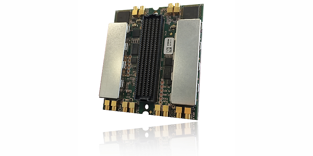
Part of this modular and flexible system concept is the proFPGA ADC Interface board. This daughter board occupies one extension site of the proFPGA system and has two 16-bit 250MSPS ADCs (ISLA216P25, Intersil). Each ADC has one channel. The two input channels of the ADCs are connected with an input filtering stage to MMCX connectors. Both ADCs are directly connected to the bottom connector. Each ADC channel has its own analog ground and a shielding. The shielding is removable for customizing the filtering circuit. 

A clock generator is on the board which sources the ADCs and 2 clock outputs. It is possible to work with the same clock for both ADCs or with different clocks. An external clock input is also connected to the clock generator which allows that one or both ADCs are working with the external clock source. An external trigger input is on the board. This port is connected to the proFPGA bottom connector and may be used for event management. The board has a proFPGA top connector which makes unused FPGA connections available to another extension board or a cable.

proFPGA ADC Interface Board
Inputs 2 differential ADC input channels (MMCX connectors), which are connected to
2 separated filtering circuits with removable shielding, which are connected to
2 ADCs (ISLA216P25, Intersil)
Clocking 1 clock generator which sources both ADCs with the identical or different clocks
2 clock outputs
1 external clock input connected to the clock generator
1 external trigger input connected to the proFPGA bottom connector
Order Code PROF-A-I-ADC

011 yes 128   產品文件:proFPGA 產品總覽 (EN) 
20171115 04   產品編號:PROF-A-I-ADC


Previous Next

Product Summary on DVI Interface Board

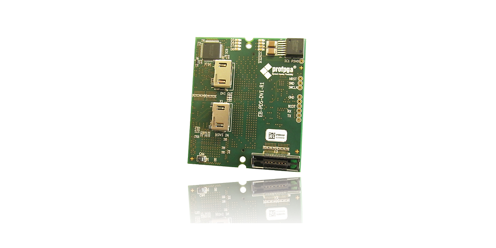
The proFPGA product family is a modular multi FPGA Prototyping solution. Part of this modular and flexible system concept is the proFPGA DVI Interface board. This daughter board occupies one extension site of the proFPGA system and provides 1 x DVI Transmitter (TI TFP410) and 1 x DVI Receiver (TI TFP403) and runs with up to 165 MHz pixel rates (including 1080p and WUXGA @ 60 Mhz. Further with DVI on board, it provides 8 x general purpose LEDs and one Mictor-38 debug connector.

proFPGA DVI Interface Board
proFPGA Connectors 1x proFPGA extension board connector (1 at bottom-side)
Interfaces 1 x DVI Transmitter (TI TFP410), 1 x DVI Receiver (TI TFP403)
Up to 165 MHz pixel rates (including 1080p and WUXGA @ 60 Mhz)
Others DVI over HDMI connectors, DVI 1.0 complient
8 x general purpose LEDs
1 x Mictor-38 debug connector
Product article number PROF049 EB-PDS-DVI-R1
Order Code PROF-A-I-DVI


011 yes 128   產品文件:proFPGA 產品總覽 (EN) 
20171115 04   產品編號:PROF-A-I-DVI


Previous Next

Product Summary

The proFPGA product family is a complete, scalable, and modular multi FPGA solution, which fulfills highest needs in the area of FPGA based Prototyping. Because of its modular and scalable system architecture, the user has maximum flexibility and reusability.

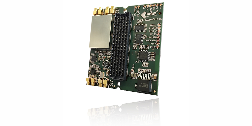
Part of this modular and flexible system concept is the proFPGA DAC Interface board. This daughter board occupies one extension site of the proFPGA system and provides a dual, 16bit digital-to-analog converter (AD9142A, Analog Devices) that supports sample rates up to 1600MSPS. Both DAC outputs are connected via analog filter stages to MMCX connectors. 

A programmable clock generator is available to provide clocks to the DAC and optionally to the FPGA and MMCX connectors. There are also MMCX connectors as a alternative clock input of the clock generator at the board. Each DAC has its own filter stage shown in Figure 146. These stages are identically for each DAC output. The implemented Low pass filter (LFCN-800+, Mini-Circuits) passes frequencies between DC and 800MHz with a maximum insertion loss of 1.3dB through. Its cut-off frequency is 990Mhz.


proFPGA DAC Interface Board
Features 1x Analog Devices AD9142A TxDAC+ DAC
16bit digital-to-analog converter that supports sample rates up to 1600MSPS
EMI shielding
Clocking programmable clock generator (configuration via proFPGA plugin)
optional clock output
optional clock input
optional clock connected to FPGAs clock capable inputs
Order Code PROF-A-I-DAC

011 yes 128   產品文件:proFPGA 產品總覽 (EN) 
20171115 04   產品編號:PROF-A-I-DAC


Previous Next

Product Summary

The proFPGA product family is a complete, scalable, and modular multi FPGA Prototyping solution, which fulfills highest needs in the area of FPGA based Prototyping. Because of its modular and scalable system architecture, the user has maximum flexibility and reusability.

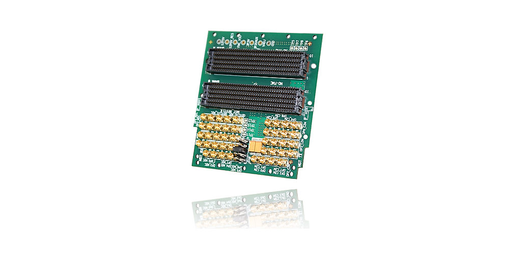
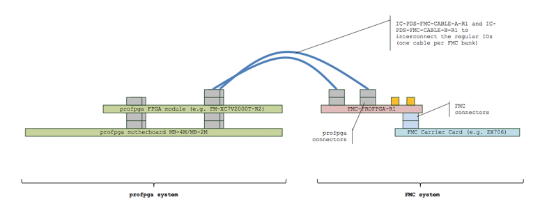
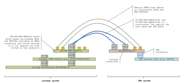
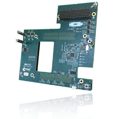
Part of this modular and flexible system concept is the proFPGA FMC Carrier Card Adapter. This daughter board occupies one extension site of the FMC carrier card and provides a connection between a FMC carrier card and the proFPGA system. It provides 2 proFPGA cable connectors (top-side), 1 FMC HPC (high pin count) connector (bottom side), 40 MMCX connectors for MGT signals (10 MGT RX and TX pairs), 4 MMCX connectors for MGT REFCLK signals (2 MGT Refclk pairs) and 1 PSU for VIO voltage generation of Bank B signals (voltage can be set via jumper). With this daughter card in combination with the proFPGA Interconnection Cables a FMC Carrier Card can easily be connected to the proFPGA system.

proFPGA System connected with FMC Carrier Card (without MGT connections)


proFPGA System connected with FMC Carrier Card (including MGT connections)


proFPGA FMC Carrier Card Adapter
proFPGA Connectors 2 proFPGA cable connectors (top-side)
FMC Connection 1 FMC HPC (high pin count) connector (bottom side)
MGT Connection 1 40 MMCX connectors for MGT signals (10 MGT RX and TX pairs,
4 MMCX connectors for MGT REFCLK signals (2 MGT Refclk pairs)
MGT Connection 2 4 MMCX connectors for MGT REFCLK signals (2 MGT Refclk pairs)
Others 1 PSU for VIO voltage generation of Bank B signals (voltage can be set via jumper)
Order Code PROF-A-MI-FMCP
011 yes 128   產品文件:proFPGA 產品總覽 (EN) 
20171115 04   產品編號:PROF-A-MI-FMCP


和澄科技 Haley Technology

電話 │ 886-3-5790380
傳真 │ 886-3-5790370
信箱 │ sales@haleytech.com
地址 │ 新竹市關新路27號18樓之2


M有任何問題嗎? Line 我們最快! 

產品搜尋