Product Summary
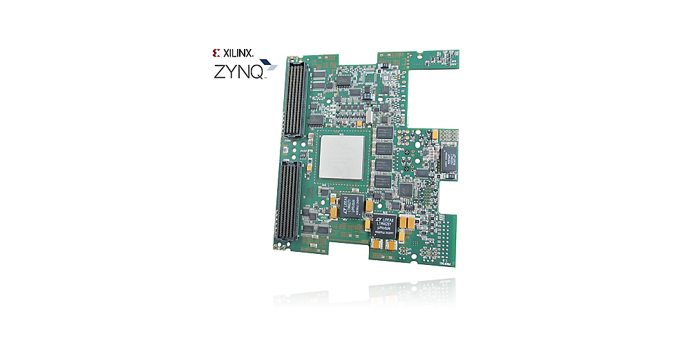
The proFPGA product family is a complete, scalable, and modular multi FPGA Prototyping solution, which fulfills highest needs in the area of FPGA based Prototyping. Part of this modular and flexible system concept is the proFPGA Zynq™ 7000 FPGA module, which can be easily mounted on the proFPGA uno, duo or quad motherboard and mixed together with various other proFPGA FPGA modules like the proFPGA Virtex 7 2000T FPGA module. The proFPGA Zynq™ 7000 FPGA module addresses customers who require a complete embedded processing platform for high performance SoC Prototyping solution, IP verification and early software development.
Equipped with a Xilinx Zynq™ XC7Z045 FPGA which combines a user FPGA with an ARM Core Processor (Dual ARM® Cortex™-A9 MPCore™ with CoreSight™) and several on board interfaces like USB 2.0 OTG, Gigabit Ethernet or ARM JTAG debug interface the Board offers a complete embedded processing platform. Further the board already 1 GB on board DDR3 and dual quad SPI flash memory.
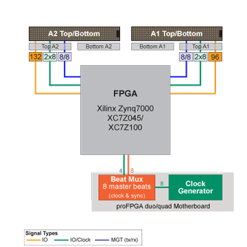
The FPGA module offers a total of 2 extension sites on the top with 260 standard I/Os and 16 high speed serial transceivers for extending the board with standard proFPGA or user specific extension boards.

| proFPGA Xilinx Zynq 7000 XC7Z045 FPGA Module Specification | |
| FPGA Type | Xilinx Zynq XC7Z045 (speedgrade 1,2 ) |
| Capacity | 2.15 M ASIC gates |
| Embedded Processor Core | Dual ARM® Cortex™-A9 MPCore™ with CoreSight™ |
| On Board Interfaces Processor Unit | USB UART interface for debugging USB 2.0 OTG Gigabit Ethernet ARM JTAG Connector for debugging PL (Programmable Logic) PS (Processing System) System reset buttons |
| On Board Memories Processor Unit | 1 GB DDR3 memory Dual Quad SPI Flash Memory |
| Signaling rate | Up to 1.2 Gbps (standard I/O)/ 12.5 Gbps (MGT) |
| Extension sites | 2 extension sites with high performance connectors |
| I/O resources | 260 per FPGA module 1 x 148 I/Os to top side connector A1 1 x 98 I/Os to top side connector A2 Single-ended or differential |
| High Speed I/O transceivers | 16 per FPGA module 1 x 8 MGTs (up to 12.5 Gb/s) to top side connector A1 1 x 8 MGTs (up to 12.5 Gb/s) to top side connector A2 |
| Available interface boards | USB 3.0, PCIe Gen2/Gen3, MIPI, DVI, DDR3 memory, Gb Ethernet, etc. |
| Voltage regions | 2 individually adjustable voltage regions per FPGA Module Stepless from 1.2V up 3.3V for HR IOs and 1.2. to 1.8 for HP IO |
| On Board Clocking | 1 x 33.333 MHz clock is generated for the ARM Core as system clock 1 x 50 MHz are provided to the FPGA PL |
| Clocking over proFPGA duo/quad Motherboard | 8 global clock and sync signal inputs per motherboard X fully synchronous derived clocks with sync signals |
| System Requirements | Works only with proFPGA uno, duo or quad motherboard |
| Configuration | JTAG interface On Board SD memory card |
| Power | External (optional) ATX Power Supply (12 V, 24 - 35 A output) |
| Dimensions | 5.91" x 0.95" x 5.91" / 150 mm x 24 mm x 150 mm (width x height x depth) 0.25 kg weight |
| Product article number | PROF061 FM-XC7Z045-R4 |
| Order code | PROF-FM-XC7Z045 |
| 產品文件:產品型錄 | |
| 產品編號:PROF-FM-XC7Z045 |


