Previous Next

記憶板 │ DDR4 5GB SDRAM Board

Product Summary

The proFPGA product family is a complete, scalable, and modular multi FPGA solution, which fulfills highest needs in the area of FPGA based Prototyping. Because of its modular and scalable system architecture, the user has maximum flexibility and reusability.

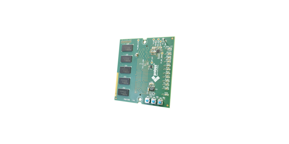
Part of this modular and flexible system concept is the proFPGA DDR4-5 SDRAM board. This daughter board occupies one extension site of the proFPGA system and offers 5 GByte DDR4 SDRAM memory and can be accessed over a 80bit databus. Due to the length matched board design, the daughter boards can be used with performances of up to 2400 Mbps. Besides the board offers three push-buttons and 8 on board LEDs, which can we used for debugging purpose.


proFPGA DDR4-5 SDRAM Board
Memory modules 5x Micron MT40A512M16HA-083E chips
Capacity 5 GB
Data rate/Databus Up to 2400 Mbps/ 80bit
Clocking programmable clock generator to create a clock for the memory generator
Others Equipped with 8 LEDs, 3 x push-buttons and ID chip for automatic board recognition
Product article number PROF069 EB-PDS-DDR4-R6
Order code PROF-A-M-DDR4-5
011 yes 128   產品文件:proFPGA 產品總覽 (EN) 
20171115 04   產品編號:PROF-A-M-DDR4-5


Previous Next

記憶板 │ Flash Board

Product Summary

The proFPGA product family is a complete, scalable, and modular multi FPGA solution, which fulfills highest needs in the area of FPGA based Prototyping. Because of its modular and scalable system architecture, the user has maximum flexibility and reusability.

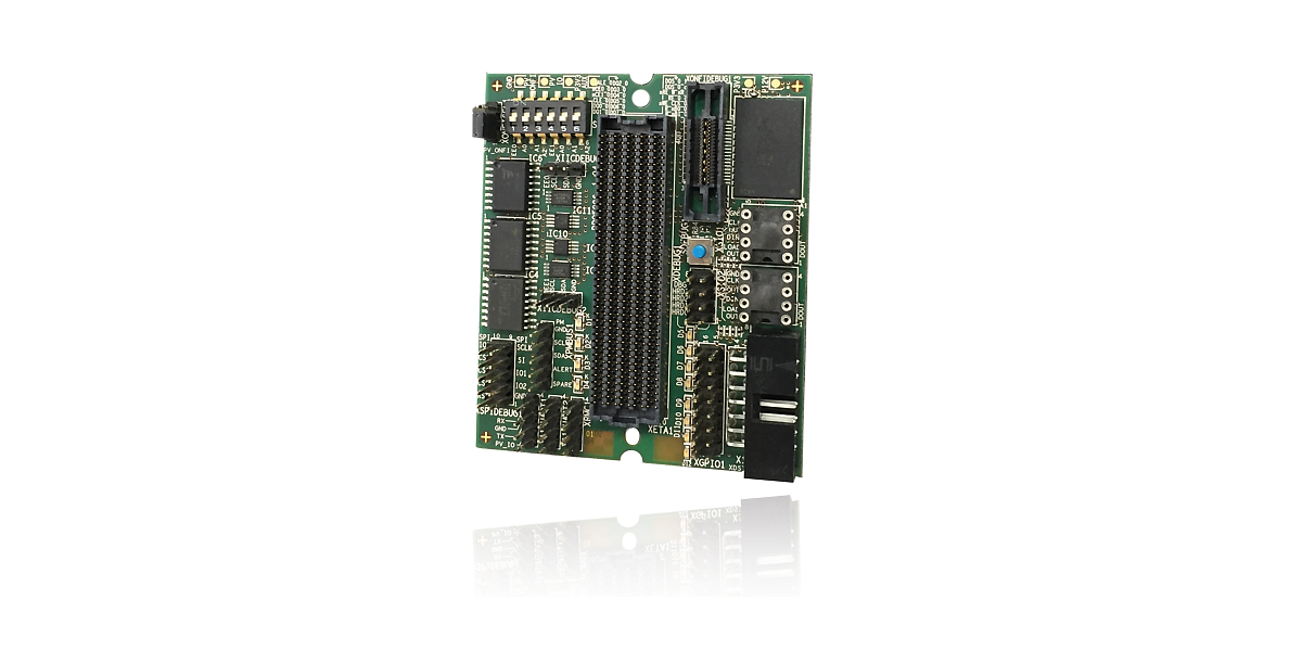
Part of this modular and flexible system concept is the proFPGA Flash board. This daughter board occupies one extension site of the proFPGA system and offers 128 Gbit ONFI flash, 512 Mbit quad SPI flash, 1 Mbit NVSRAM, 1 Mbit quad SPI MRAM, Debug interface for ONFI flash with 38-pin MICTOR connector, debug interface for all SPI signals of all SPI devices, 2 x I²C 64 kbit EEPROMs, 1 x debug interface for each I²C EEPROM, I²C EEPROM address selection via DIP switch, 1 x A15 Dstream connector, 1 x PMBus header, 3 x UART headers, 1 x heartbeat LED, 3 x debug LEDs, 1 x push button, debug header with 4 IO signals connected with pull-ups and the possibility to assemble jumpers to set a low input signal and a debug header with 8 IO signals connected with pull-ups, the possibility to assemble pull-downs and the possibility to assemble jumpers to set a low input signal. Additionally green LEDs are connected to each GPIO line.

proFPGA Flash Board
Memory modules 128 Gbit ONFI flash (MT29F128G08AMCDBJ5-6)
512 Mbit quad SPI flash (S25FL512SAGMFI011)
1 Mbit NVSRAM (CY14V101Q3)
1 Mbit quad SPI MRAM (MR10Q010SC)
Debug Interface Debug interface for ONFI flash with 38-pin MICTOR connector
Debug interface for all SPI signals of all SPI devices
Debug interface for each I²C EEPROM
3 x debug LEDs
Debug header with 4 IO signals
Debug header with 8 IO signals
Green LEDs are connected to each GPIO line.
Others 2 x I²C 64 kbit EEPROMs (AT24C64D-XHM-T)
I²C EEPROM address selection via DIP switch
1 x A15 Dstream connector
1 x PMBus header
3 x UART headers
1 x heartbeat LED
1 x push button for user usage
Product article number PROF086 EB-PDS-FLASH-R1
Order code PROF-A-M-ONFL
  產品文件:proFPGA 產品總覽 (EN) 
  產品編號:PROF-A-M-ONFL


Previous Next

記憶板 │ LPDDR4 Board

Product Summary

The proFPGA product family is a complete, scalable, and modular multi FPGA solution, which fulfills highest needs in the area of FPGA based Prototyping. Because of its modular and scalable system architecture, the user has maximum flexibility and reusability.

Part of this modular and flexible system concept is the proFPGA LPDDR4 board. This daughter board occupies one extension site of the proFPGA system and offers with 2x Samsung K4F8E304HB-MGCJ memory devices 2 GByte LPDDR4-3200 capacity. Besides the board offers three push-buttons and 3 on board LEDs.

Northwest Logic's full-featured, high-efficiency LPDDR4 SDRAM Controller Core is verified for the Virtex UltraScale based proFPGA platform and LPDDR4 Memory Boardsolution and utilizing Northwest Logic's proprietary FPGA-based LPDDR4 PHY.

proFPGA LPDDR4 Board
Memory modules 2x Samsung K4F8E304HB-MGCJ Chips
Capacity 2 GB
Verified Controller and PHY Northwest Logic's LPDDR4 SDRAM Controller Core and proprietary FPGA-based LPDDR4 PHY
Compatibility Works with all available proFPGA Xilinx Virtex UltraScale basedFPGA Modules
Others Equipped with 8 LEDs and 3 x push-buttons
Product article number PROF117 EB-PDS-LPDDR4-R1
Order code PROF-A-M-LPDDR4
  產品文件:proFPGA 產品總覽 (EN) 
  產品編號:PROF-A-M-LPDDR4


Previous Next

記憶板 │ LPDDR2 Board

Product Summary

The proFPGA product family is a complete, scalable, and modular multi FPGA solution, which fulfills highest needs in the area of FPGA based Prototyping. Because of its modular and scalable system architecture, the user has maximum flexibility and reusability.

Part of this modular and flexible system concept is the proFPGA LPDDR2 board. This daughter board occupies one extension site of the proFPGA system and offers 2x two GBit Winbond W97BH2KBQX memory devices which can be accessed over a 32bit databus. Due to the length matched board design, the daughter boards can be used with performances of up to 800 Mbps. Besides the board offers three push-buttons, 16 on board LEDs and 2 SoftTouch connectors, which can we used for debugging purpose.

proFPGA LPDDR2 Board
Memory modules 2x two GBit Winbond W97BH2KBQX devices
Capacity 0.5 GB
Data Rate Up to 800 Mbps
Memory organization 32 bit x 64M
Others Equipped with 16 LEDs, 3 x push-buttons and 2 SoftTouch connectors
Product article number PROF084 EB-PDS-LPDDR2-R1
Order code PROF-A-M-LPDDR2
  產品文件:proFPGA 產品總覽 (EN) 
  產品編號:PROF-A-M-LPDDR2


Previous Next

記憶板 │ Multi Memory Board

Product Summary

The proFPGA product family is a complete, scalable, and modular multi FPGA solution, which fulfills highest needs in the area of FPGA based Prototyping. Because of its modular and scalable system architecture, the user has maximum flexibility and reusability.

Part of this modular and flexible system concept is the proFPGA Multi Memory board. This daughter board occupies one extension site of the proFPGA system and provides 3 different types of memory with several debug opportunities like: 16 Mbit SRAM (CY62167EV18), 256 Kbit MRAM (MR256D08B), 512 Mb NOR Flash (JS28F512M29EWHA), 2x Buttons for debugging, 4x LEDs (green, red, yellow, blue) for debugging, 4x 1.8V GPIO-Pins for debugging, 2x MICTOR Connectors for debugging, DIP-SWITCH for changing Pull-Ups and -Downs for some address-pins and level shifters for operating independent from PVIO.

proFPGA Multi Memory Board
Memory type SRAM 16 Mbit SRAM (CY62167EV18)
Memory type MRAM 256 Kbit MRAM (MR256D08B)
Memory type NOR Flash 512 Mb NOR Flash (JS28F512M29EWHA)
Interfaces 2x MICTOR Connectors; 4x 1.8V GPIO-Pins
Others Equipped with 4 LEDs, 2 x push-buttons, DIP-SWITCH for changing Pull-Ups and -Downs
Order code PROF-A-M-MUME
  產品文件:proFPGA 產品總覽 (EN) 
  產品編號:PROF-A-M-MUME