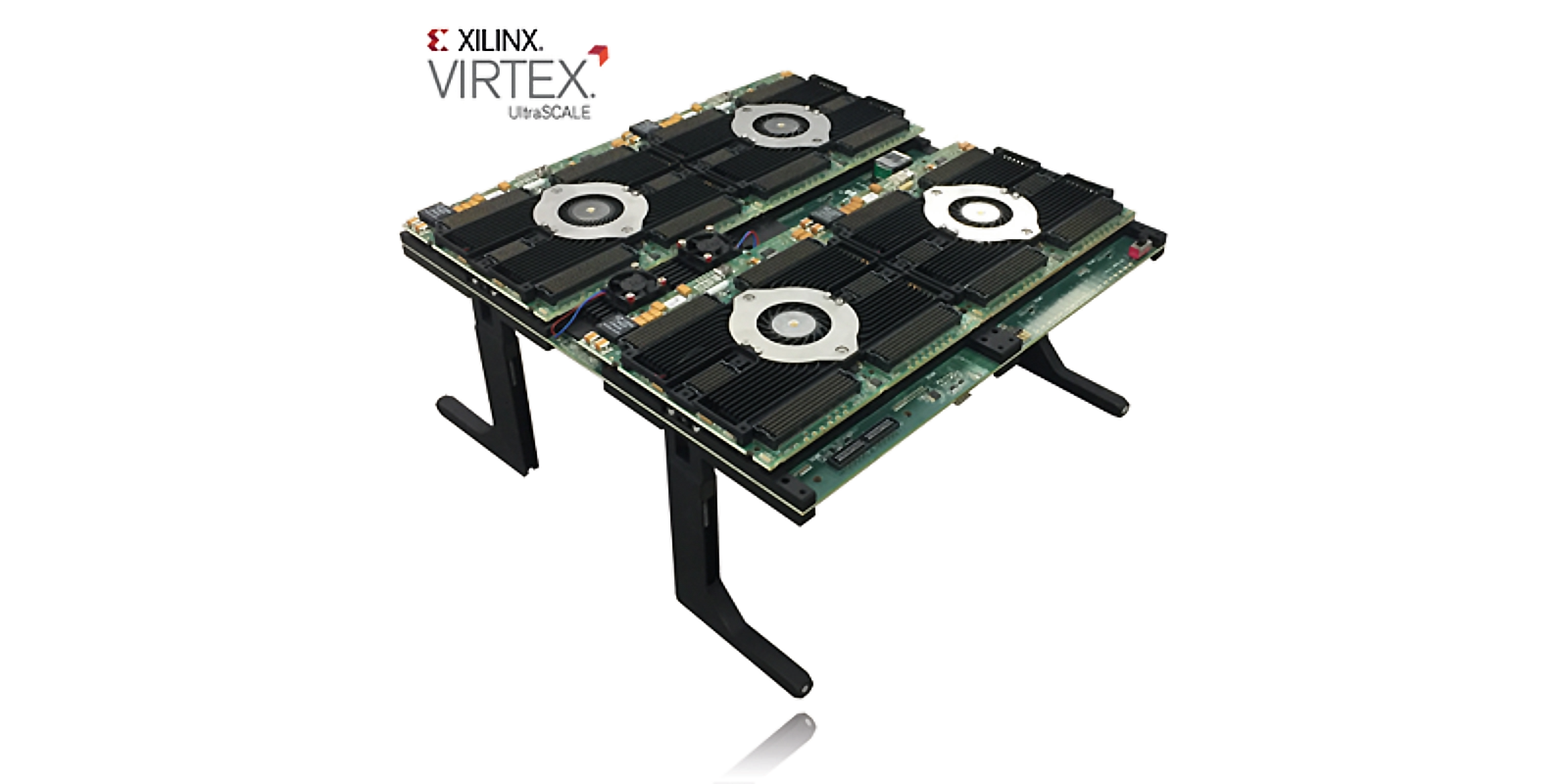
UltraScale Prototyping System
UltraScale Prototyping System - The proFPGA quad VUS 440 system is a complete and modular multi FPGA solution, which meets highest requirements in the area of FPGA based Prototyping. It addresses customers who need a scalable and flexible high speed ASIC Prototyping solution for early software development and real time system verification. The innovative system concept offers highest flexibility and reusability, reconfigurability for several projects, which guarantees the best return on invest.rn on invest.
Highest Flexibility
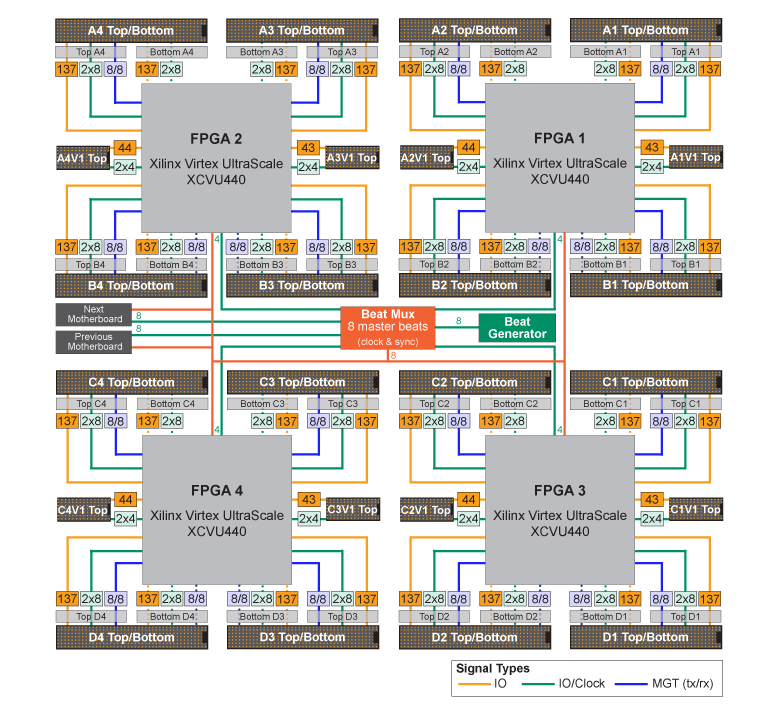
The system architecture is based on a modular and scalable system concept. The FPGAs are assembled on dedicated FPGA modules, which will be plugged on the proFPGA uno, duo or quad mother board. This offers the highest flexibility to use for example different FPGA types in one system or to scale a system in increments of one FPGA. The user has nearly 100% access to all available I/Os of the FPGA, which gives him maximum freedom regarding the FPGA inter connection structure. This way the prototyping system can be adapted in the best way to any user design. Furthermore the system offers a total of 40 extension sites on the top and bottom site for standard proFPGA or user specific extension boards like DDR-4 memory, PCIe gen1/2/3, Gigabit Ethernet, USB 3.0 or other high performance interface and interconnection boards.
Maximum Performance
The well designed boards of the proFPGA system are optimized and trimmed to guarantee best signal integrity and to achieve highest performance. The high speed boards together with specific high speed connectors allow a maximum point to point speed of up to 1.0 Gbps single ended over the standard FPGA I/O and up to 12.5 Gbps differential over the high speed serial transceivers of the FPGA. This performance combined with the high interconnection flexibility allows the designer to run his design at maximum speed in the proFPGA system.
Big Capacity
Equipped with up to 4 Xilinx Virtex® UltraScale™ 440 FPGA modules, the proFPGA quad system can handle up to 120 M ASIC gates on only one board. Due to the fact, that multiple proFPGA quad or duo systems can be connected to an even larger system, there is an unli- mited scalability and no theoretical maximum in capacity.
Very User Friendly
The proFPGA prototyping system provides an extensive set of features and tools, like remote system configuration, integrated self and performance test, automatic board detection, automatic I/O voltage programming, system scan and safety mechanism, which simplifies the usage of the FPGA based system tremendously.
Specification
FPGAs
- Up to 4 x Xilinx Virtex® XCVU440 FPGA Modules
Capacity
- Up to 120 Million ASIC gates on one board (30 Million ASIC gates per FPGA Module)
FPGA-internal memory
- Up to 354,400 kbits on one board (88,600 kbits per FPGA Module)
Signaling rate
- Up to 1.0 Gbps single ended (standard I/O)/ up to 12.5 Gbps (MGT) differential
Extension sites
- Up to 40 extension sites with high speed connectors
I/O resources
- Overall 5308 signals for I/O and inter FPGA connection
- 1327 free I/Os per FPGA Module
- 4x153 I/Os and 1x52 I/Os and 1x51 I/Os to top side connectors
- 4x153 I/Os to bottom side connectors
- Single-ended or differential
High Speed I/O transceivers
- 192 dedicated MGTs running up to 16 Gbps
- 48 MGTs (up to 12.5 Gbps) per FPGA Module
FPGAs interconnections
- Flexible via high-speed interconnection boards or cables
Voltage regions
- 40 individually adjustable I/O voltage regions
- 10 individually adjustable voltage regions per FPGA Module
- Stepless from 1.0V up to 1.8V on 9 extension sites, from 1.0V up to 3.3V on one extension site
- Automated detection of daughter card and adjustment of right voltage
Configuration
- With host software via Ethernet, USB 2.0, PCIe or standalone over USB stick or JTAG
Clock Management
- 288 differential external clock inputs
- 72 differential clock inputs per FPGA Module
- 8 differential clock inputs per connector
- 4 external clock/sync inputs/outputs over HF SMA connectors
- Run-time configurable local clocks
- 8 global clock and sync signal inputs per motherboard
- Fully synchronous derived clocks with sync signals
Data exchange
- On board DMBI (Device Message Box Interface)
Data exchange rate:
- Ethernet (up to 100 Mbps)
- USB (480 Mbps)
- PCIe (up to 3.5 Gbps)
Power
- External (optional) ATX Power Supply (12 V, 24 - 35 A output)
Dimensions
- 11.81" x 0.95" x 12.20" / 300 mm x 24 mm x 310 mm (width x height x depth)
- 2.5 kg weight
System Architecture
| proFPGA quad UltraScale XCVU440 FPGA Prototyping System Configurations | ||||
| proFPGA quad VUS FM1 | proFPGA quad VUS FM2 | proFPGA quad VUS FM3 | proFPGA quad VUS FM4 | |
| Extension Sites | 10 | 20 | 30 | 40 |
| FPGA Modules | 1 | 2 | 3 | 4 |
| FPGAType | Xilinx Virtex XCVU440 | Xilinx Virtex XCVU440 | Xilinx Virtex XCVU440 | Xilinx Virtex XCVU440 |
| Logic Capacity (ASIC Gates) | 30 M | 60 M | 90 M | 120 M |
| FPGA Memory | 88,600 kbits | 177,200 kbits | 265,800 kbits | 354,400 kbits |
| I/O Resources | 1327 | 2654 | 3981 | 5308 |
| High Speed I/O Transceivers | 48 | 96 | 144 | 192 |
| Adjustable Voltage Regions | 10 | 20 | 30 | 40 |
| Interconnections | flexible | flexible | flexible | flexible |
| Clock Inputs | 72 + 4 | 144 + 4 | 216 + 4 | 288 + 4 |
| Global Clocks | 8/x-derived | 8/x-derived | 8/x-derived | 8/x-derived |
| Order Code | PROF-QUAD-VUS-FM1 | PROF-QUAD-VUS-FM2 | PROF-QUAD-VUS-FM3 | PROF-QUAD-VUS-FM4 |
| 產品文件:產品型錄(EN) │proFPGA 產品總覽 (EN) |
|
| 產品編號:PROF-QUAD-VUS-FM1, PROF-QUAD-VUS-FM2,PROF-QUAD-VUS-FM3, PROF-QUAD-VUS-FM4 |